Thermal Infrared Spectrometer MERTIS for The Bepicolmbo Mission To Mercury

Zeh, T(1); Kaiser, S.(1); Lenfert K.(1); Peter, G.(2); Walter, I.(2); Hirsch, H.(2); Knollenberg, J.(2); Helbert, J.(2); K. Multhaup(3), H. Hiesinger(3); Gebhardt, A.(4); Risse, S.(4); Damm, C.(4); Eberhardt, R.(4); Baier, V.(5); Keßler, E. (5)
(1)Kayser-Threde GmbH, Wolfratshauser Straße 48, 81379 München, Germany, [email protected] (2)Deutsches Zentrum für Luft- und Raumfahrt (DLR), Rutherfordstraße 2, 12489 Berlin, Germany (3)Institut für Planetologie, Wilhelm-Klemm-Str. 10, 48149 Münster, Germany
(4)Fraunhofer-Institut für angewandte Optik und Feinmechanik, Albert-Einstein-Str.7, 07745 Jena, Germany
(5)Institute of Photonic Technology e.V., Albert-Einstein-Straße 9, 07745 Jena, Germany
ABSTRACT
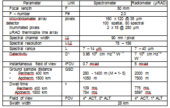
The MERTIS instrument is a thermal infrared imaging spectrometer onboard of ESA’s cornerstone mission BepiColombo to Mercury. MERTIS will provide detailed information about the mineralogical composition of Mercury’s surface layer by measuring the spectral emittance in the spectral range from 7-14
µm with a high spatial and spectral resolution. Furthermore MERTIS will obtain radiometric measurements in the spectral range from 7-40 µm to study the thermo-physical properties of the surface material. Under the lead of the German Aerospace Center DLR (Dep. Optical Information Systems, Berlin) a development model (DM) is in development which integrates all MERTIS sub-units of later flight models. With the DM the general design and performance goals of the system shall be investigated and verified. Besides a general overview about the instrument principles the following topics are addressed: Optics setup with a Three Mirror Anastigmatic (TMA) telescope and Offner Spectrometer, Manufacturing techniques for the robust and high precision optics and Radiometer Concept and Design
1. INTROCUCTION
The recent knowledge about the infrared spectral emittance of Mercury’s surface is limited to a number of ground-based telescopic studies e.g. [6], [7] or data from Mariner 10 [8] which flew past Mercury three times in 1974 and 1975. Several studies suffer from their restriction to the NIR-range, where pure feldspars have no specific spectral signature [9]. In the Thermal Infrared (TIR), however, feldspars can be detected by means of their diagnostic spectral signatures: Christiansen frequency, reststrahlen band, and transparency feature. In addition, pyroxenes and most other minerals can be detected and specified in this spectral range. Thermal infrared spectroscopy operating in the range between 7 and 14 µm will enable valuable mineral identification of feldspars and low-iron species that are expected to be prevailing on Mercury’s surface. Performing TIR measurements will make it possible to identify spectral features associated with the high radar backscattering efficiency of putative minerals and to differentiate between the proposed compositions (water ice, sulphur, and cold silicate glasses) for the high- latitude volatiles, something that cannot be done by ground based observing or near-infrared spectroscopy. [9]. In summary, MERTIS has four scientific goals: the study of Mercury’s surface composition, identification of rock-forming minerals, mapping of the surface mineralogy, and the study of the surface temperature variations and thermal inertia. The instrument will provide detailed information about the mineralogical composition of Mercury’s surface layer by measuring the spectral emittance in the spectral range from 7-14 µm with a high spatial and spectral resolution [1], [2], [3]. Furthermore MERTIS will obtain radiometric measurements in the spectral range from 7-40 µm to study the thermo-physical properties of the surface. MERTIS is a joint project of the Institut für Planetologie (IfP) at the Westfälische Wilhelms- Universität (WWU) Münster, two institutes of the German Aerospace Center (DLR) in Berlin-Adlershof and several industrial partners and research institutes.
2. INSTRUMENT OVERVIEW
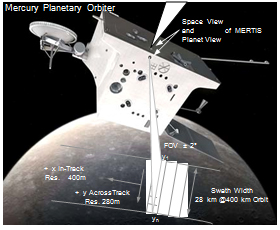
The MERTIS instrument is an IR-imaging spectrometer and radiometer working on a high resolution push- broom principle. The spectrometer employs an un- cooled microbolometer array made from amorphous silicon, which yields a short thermal time constant as well as very low noise equivalent temperature difference NETD [10]. The array provides spectral separation and spatial resolution according to its two- dimensional shape. The operation concept principle is characterized by intermediate scanning of the planet surface and three different calibration targets – free space and on-board black body sources. Sharing the same optical path a push-broom radiometer is implemented according an in-plane separation arrangement.
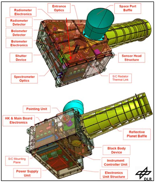
The general instrument architecture comprises two separate parts – the Sensor Head including optics, detector and proximity electronics and the Electronics Unit containing the power supply with an interface to the primary bus, the sensor control and the driving electronics. This highly integrated and with 3.3 kg extreme light weighted measurement system is completed by a motor driven Pointing Unit device which orients the optical path to the planet and the calibration targets. The following figures give an overview on the instrument configuration.
3. OPTICS SETUP
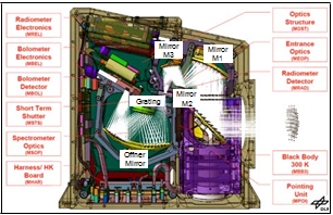
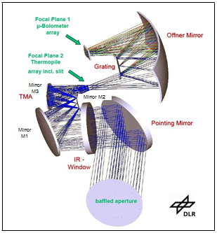
The design is based on an all-reflective optics concept with an off-axis Three Mirror Anastigmatic (TMA) telescope behind an IR entrance window and a pointing mirror for the target selection (planet view or calibration views to deep space and two reference sources). The spectrometer is a derivative of an elegant relay disclosed by Offner in the early 1970’s [6]. This combination is free from spherical aberration, coma and distortion and, when the algebraic sum of the powers of the mirror reflecting surfaces utilized is zero, the image produced is free from third order astigmatism and field curvature [6].
4. OPTICS MANUFACTURING
4.1. Manufacturing Goals
The MERTIS reflective infrared optics for the spectral range from 7-14 µm can be ideally implemented as diamond turned aluminium mirrors coated with a thin gold layer. Single Point Diamond Turning (SPDT) offers the possibility to manufacture both, the optical surface and mechanical references in close tolerances and in respect to each other. From the manufacturing point of view the MERTIS optics consists of three different mirror types:
– On-axis mirrors: M2, Offner mirror
– Off-axis mirrors: M1, M3
– Spherical grating: Offner grating
For all elements mechanical simulations were carried out for an optimization regarding:
– Minimizing mounting forces during manufacturing and assembly.
– Minimizing centrifugal forces during SPDT.
The usage of identical reference planes on the mirror bodies for alignment during manufacturing, measurement and system assembly was an essential approach.
4.2. On-axis Mirrors
The on-axis mirrors M2 and the Offner mirror can be fabricated using the traditional diamond turning process. Due to interferometric measurements and following correction loops the figure deviation of the M2 mirror is reduced to around 100 nm p.-v.. Due to the usage of a novel aluminium alloy with refined grain size the surface roughness is less than 4 nm RMS (measurement area 315 µm x 235 µm) [4].
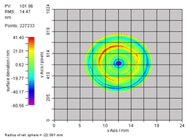
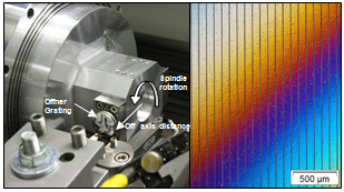
Сonsidering the simulation results of the light weight structure regarding the deformation under rotation, the spindle speed was reduced to 400 rpm for the Offner mirror. By turning the mirror with the calculated spindle speed a typical figure deviation of less than 300 nm p.-v. has been achieved for the Offner mirror. The radius of curvature and the vertex height can be manufactured in a tolerance of 0.01 mm.
4.3. Off-axis Mirrors
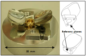
The M1 and M3 mirrors are similar excepting their size and will be fabricated in the same manner. The mirror bodies are mounted on a fixture, well referenced using a central dowel pin and clamps. After SPDT the guide edges of the fixtures are measured with a coordinate measuring machine. Together with the Z-position of the last cut this data provides the position (X,Y,Z) of the optical surface with respect to the mirror reference planes. This knowledge is essential for a deterministic alignment on the TMA optics.
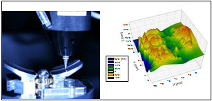
Because of the deviation of the M1 and M3 aspheres from the best fit sphere it is not possible to measure the M1 and M3 interferometrically without a Computer Generated Hologram (CGH). An alternative solution is the usage of a tactile 3-D profilometer to measure the surface shape. Because of the risk of scratches due to the cantilever the final tactile measurements has to be done before the last cut.
4.4. Spherical Grating
Rotationally symmetric microstructures like blazed gratings can easily be cut into flat, spherical or aspherical substrates by diamond turning. Cutting a linear grating in a spherical substrate is more difficult – but possible as well. In case of the Offner grating the substrate is mounted in an off-axis position with a distance equal to the radius of curvature of the desired sphere. This technique is typically used for the manufacturing of toroids. In case of the Offner grating the toroid has two identical radii. One radius of curvature is build by the off axis distance and the second radius of curvature is build by the tool path. The tool path can include a grating structure and other shaped elements.
4.5. Coating
After a cleaning procedure the mirrors were immediately coated with gold. The thin film deposition is a sputtering process to achieve a good adhesion and durability of the coating. The gold coating withstand requirements accordingly to
− Adhesion test, Procedure:Tapetest DIN 58196-6
− Humidity, Procedure:MIL-M-13508C 4.45 (49°C / 95% RH/ 24 h)
− Temperature change, Procedure:ISO 9022-2-14-04 (-50/+60 °C, 5 cycles, 30% humidity)
The reflectance of the gold coating on the diamond turned mirrors rises up from 97.5 % @ 1000nm to more than 98.5 % fore wavelength above 2000 nm.
5. OPTICS VERIFICATION (TMA)
Figure 5-1 illustrates the assembly principle of the TMA optics. The TMA-housing contains a central hole representing the optical axis. The M2 mirror and a dowel pin are fixed in this hole. The adjustment of M1 and M3 is done by gauge blocks in X- and Y- direction and by assembly plates in Z-direction (respectively in Rx and Ry). Furthermore well-known are:
– The position of the mirrors reference planes in respect to the aspheres
– The vertex positions of M1, M2, M3
– The mirror radii
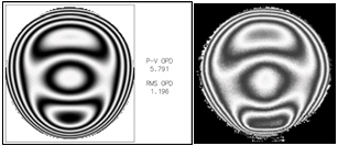
The manufacturing of the housing is done according to these measures values from the mirrors. The outcome is an initial TMA assembly, which creates a wave front image that can be improved by interferometric observation.

5.2. TMA verification
The optical alignment of the TMA is done by an iterative process. Based on the initial wave front data new positions and tilt angles of M1 respectively M3 are calculated with optical design tools. These movements are realized by custom gauge blocks and plates. In this way the TMA was aligned close to the theoretical wave front.
6. MERTIS RADIOMETER
6.1. Technical Concept and Design
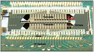
The basic concept of the proposed MERTIS radiometer channel is to place a 2×15 elements thermopile double line array sensor chip with integrated optical slit for the spectrometer at the focal plane of the TMA entrance optics. The small signal voltages of the order of µV to mV generated by the thermopile sensors are transmitted differentially via a starr-flex interface PCB to a proximity electronics, where the signals are multiplexed, amplified, converted to digital units and transmitted to the MERTIS ICU.
The unusual solution of incorporating the optical slit into the radiometer chip was driven by the very small space available which is mainly a consequence of the MERTIS requirement to minimize the heat input through the entrance optics. This design requires a modification of the standard thermopile design where a self-supporting membrane containing the thermoelectrically active layers is spanned over a surrounding Si frame. Here, an additional central bridge is added to the Si frame which provides additional mechanical support (see figure below), thereby allowing to cut the slit into the center of the membrane. Furthermore, the thermopile pixels are only weakly coupled to this central Si bridge by very narrow V- shaped bars to reach the maximum possible sensitivity.
Each thermopile pixel of 200 x 1100 µm size consists of 14 thermocouples connected in series using Bi0.87Sb0.13/Sb as thermoelectric materials. The pixels are coated by a thin layer of black silver smoke, a material with nearly constant high absorption from the visible to the far infrared. The pixel width of 200 µm is close to the diffraction limit of the optics at 40 µm wavelength, a small gap of 50 µm width between the pixels is necessary for technological reasons and also effectively eliminates thermal crosstalk between neighboring pixels (under vacuum).
One infrared 8-14 µm bandpass filter is mounted directly above the thermopile array on 50 µm high standoffs which are micro machined directly onto the chip. The other array uses only the MERTIS entrance filter to realize a 7-40 µm broadband IR channel which is aimed at measuring low object temperatures down to 100 K.
The electrical interface of the thermopile arrays is provided by direct wire bonding of the sensor signals to a starr-flex PCB, the ends of the two flex wires are equipped with a Nano-connector to feed the signals into the radiometer electronics. Chip and PCB are mounted inside a dedicated Aluminum housing comprising of a baseplate and a cover. The whole detector unit is then fixed to the TMA structure by Shapal spacers which are providing an excellent thermal coupling but electrical insulation.
6.2. Manufacturing and Verification
For the manufacturing of the detector chips 300 µm thick wafers of <110> Si equipped with a 1 µm thick Si3N4 membrane were chosen. The process starts with the anisotropic deep etching of the Si to create the support frame and the staircase structure in the centre. The next steps are devoted to the microstructuring of the thermopile functional layers (Bi0.87Sb0.13, Sb, isolation and passivation layers) into the membrane. After cutting the wafer into individual chips the processing continues on single chip level with the manufacturing of the 50 µm wide optical slit by reactive ion etching. The last step to finalize the detector chip is the deposition of the black silver smoke absorber through a micro machined aperture. The necessary backside cover which is required to prevent straylight (note that the detector chip is partly transparent to infrared light) to enter the spectrometer part of MERTIS is realized as a 10 µm thick copper foil glued onto the rear side of the detector. Into the central part of this foil a 500 µm wide slit of 4 mm length is etched to guarantee an unobstructed field-of-view for the radiation passing the optical slit (the 50 µm wide slit etched into the thermopile membrane) of the spectrometer.
The whole chip ensemble is glued to an Aluminium baseplate of 0.8 mm thickness which acts as a heat sink. To allow reliable bonding from the thin detector chip (300 µm) to the thicker (800 µm) PCB a pedestal of 500
µm height is added to the central part of the baseplate. Furthermore, the pedestal is equipped with two mounting edges which allow the positioning of the chip (especially the slit) to a few micron accuracy, a requirement which stems from the optical alignment strategy. All Aluminium parts of the housing are coated with Fractal Black [11].
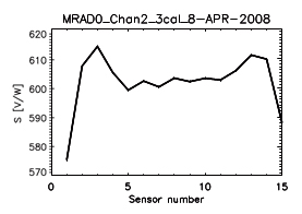
The performance of the thermopile arrays was verified by mounting the detector inside a vacuum chamber and looking through a KRS-5 window onto an external blackbody. By varying the temperature of the blackbody between 20°C and 80°C an average sensitivity of about.
600 V/W could be derived (see Fig. 5-2). The inhomogeneity of the array is less than 2%, except for the two outermost pixels because they are slightly better coupled to the Si frame which acts as a heat sink. With thermopile resistances in the range of 28-30 kOhms these numbers correspond to an average detectivity of about 1.3 109 cm Hz1/2 W-1 , a value which is 30% better than the design goal.
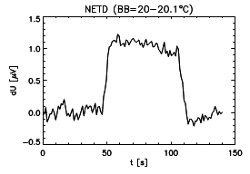
Furthermore, the NETD of the radiometer system (detector + front-end-electronics) has been measured in a MERTIS-like configuration where the TMA was replaced by a f/2.2 ZnSe lens. Here, the increase of the blackbody temperature be 0.1°C causes an increase of 1.1 µV in the thermopile voltage. Comparison to the noise level of about 70 nV gives a NETD=6 mK at room temperature. This value is consistent with NETD < 0.5 K at the minimum design target temperature of 100 K, thus fulfilling the MERTIS requirements.
CONCLUSION
We showed that the concept, design and so far obtained performance of the optical sub-units of the MERTIS DM can be regarded as appropriate and for the later flight models. Up to now the components have been tested and verified only on sub-unit level. Currently in work is their integration into the complete instrument in order to investigate mutual influence and interferences and to verify the performance of the complete instrument. The results we have obtained so far are promising for this integration and verification phase.
ACKNOWLEDGEMENTS
MERTIS is a joint project of the Institut für Planetologie (IfP) at the Westfälische Wilhelms- Universität (WWU) Münster and two institutes of the German Aerospace Center (DLR) in Berlin-Adlershof, as well as several industrial partners, including Kayser- Threde GmbH München. The MERTIS instrument, funded by the Federal Government of Germany through the German Space Agency, is part of the scientific payload of the BepiColombo mission to Mercury. This mission is developed by the European Space Agency (ESA) in close collaboration with Japan.
REFERENCES
- MERTIS – A Thermal infrared imaging spectrometer for the Bepi-Colombo mission, Internet: https://solarsystem.dlr.de/TP/MERTIS_en.shtml
- Uncovering the secrets of Mercury, Internet https://www.uni-muenster.de/Planetology/science/projects/mertis/index.html
- BepiColombo overview, Internet: https://www.esa.int/Science_Exploration/Space_Science/BepiColombo_overview2
- Gubbels, G. et al, Rapidly solidified aluminium for optical applications; SPIE Proc., Marseille 2008
- Offner, A. : UNIT POWER IMAGING CATOPTRIC ANASTIGMAT, United States Patent 3748015, July 24, 1973
- Sprague, A. L., Roush, T. L., Comparison of Laboratory Emission Spectra with Mercury Telescopic Data. In: Icarus, Vol. 133, Issue 2, pp. 174-183,1998.
- Cooper, B. et al: Midinfrared spectra of Mercury. In: JOURNAL OF GEOPHYSICAL RESEARCH, VOL. 106, 2001 NO. E12, PAGES 32,803–32,814
- Hapke, B., Danielson, G.E., Jr., Klaasen, K., Wilson, L.: Photometric observations of Mercury from Mariner
- J. Geophys. Res. 80, 2431–2443, 1975
- Benkhoff ,J; Helbert, J.:Thermal infrared spectroscopy to investigate the composition of mercury – The MERTIS instrument on BepiColombo. In: Advances in Space Research, Volume 38, Issue 4, 2006, Pages 647-658, Published by Elsevier Ltd.
- W. Rabaud; M. Vilain; J. Meilhan; T. Garret; G. Hopkinson; M. S. Bentley; S. Kraft; O. Legras; P. Castelein: Uncooled detector development for space application . SPIE Proceedings Vol. 6958, Sensors and Systems for Space Applications II, , 2008, DOI:10.1117/12.777993
- Acktar Ltd., 1 Leshem St, Entrance A, P.O.B. 8643; Kiryat-Gat 82000, Israel